Hybrid plasmonic waveguide for on-chip photonic devices
From phones to tablet computers, fast processing of information is central to modern society. This task is traditionally carried out by electronics, however this is becoming too slow and energy-consuming. Among alternative technologies, photonics is the most promising, because it is fast, energy efficient and compact, but possible photonics solutions are either still too bulky or suffer from high ohmic losses when light travels through metallic structures, necessary to bring light to the nanoscale. By combining metals merely to confine light, and dielectrics as lossless waveguides, a “hybrid” device thus avoids the drawbacks of traditional photonic solutions.
Fast transfer and processing of information are crucial to our modern society. They are mostly carried out by a combination of electronics, for processing the information and converting the outcome into light signals, and photonics, for transmitting those light signals over long distances via optical fibres. However, these traditional roles are not enough to fulfil the increasing demands for more and more information. Electronics equipment has become increasingly the bottleneck because of its bulkiness, its high power dissipation and consumption, its slow processing capabilities, and its vulnerability to electromagnetic interference. Light-based devices are taking over some of its tasks such as the transfer of information between different circuit boards in large computers (interconnects), and the on-chip processing of information, rather than just its transfer. Photonics is attractive because photonic devices can respond very rapidly, are immune to electromagnetic interference, have very low power dissipation, and allow for parallel processing. Being able to take over some tasks from electronics requires light to interact with itself, which does not happen at low light intensities. If the light intensity in an appropriate material becomes high enough, it interacts with itself, generating, for instance, new colours (frequencies). These nonlinear phenomena are thus light intensity dependent.
Nonlinear optical effects are very weak. Two approaches have been explored to exploit substantial nonlinear phenomena: (i) transparent materials like glasses or semiconductors (photonics), which cannot compress light more than half a wavelength and thus require long propagation distances, leading to large linear dimensions; (ii) opaque, absorbing materials like metals (plasmonics), which can enormously compress light, giving rise to huge light intensities, so long propagation lengths are not required, leading to compact structures. However, the high losses tend to prevent this approach from reaching its full potential.
The overall goal of this research project is to explore, through modelling and experiment, an alternative approach which combines the best characteristics of metals and dielectrics into a hybrid structure, which exhibits high light intensities, moderate losses and on-chip compatibility.
The basic structure of every on-chip photonic device is a waveguide. Therefore our basic hybrid structure is a waveguide made of a nonlinear dielectric material (core), sandwiched between a metallic layer (plasmonic structure) and another dielectric material, which exhibits high nonlinearities. We call this a hybrid plasmonic waveguide (HPWG). Hybrid plasmonic architectures combine the best characteristics of traditional photonics and plasmonics, and can strongly confine the field. Such high confinement leads to huge optical intensities, so that strong nonlinear effects result. Critically, the structure can be engineered for larger nonlinear effects than in pure photonic structures with lower losses than in pure plasmonic devices. Hence, HPWGs can be the keystone for future on-chip photonic signal processing and nonlinear optical devices as well as quantum information processing.
This research was funded by the ARC Discovery Project (DP150100779)
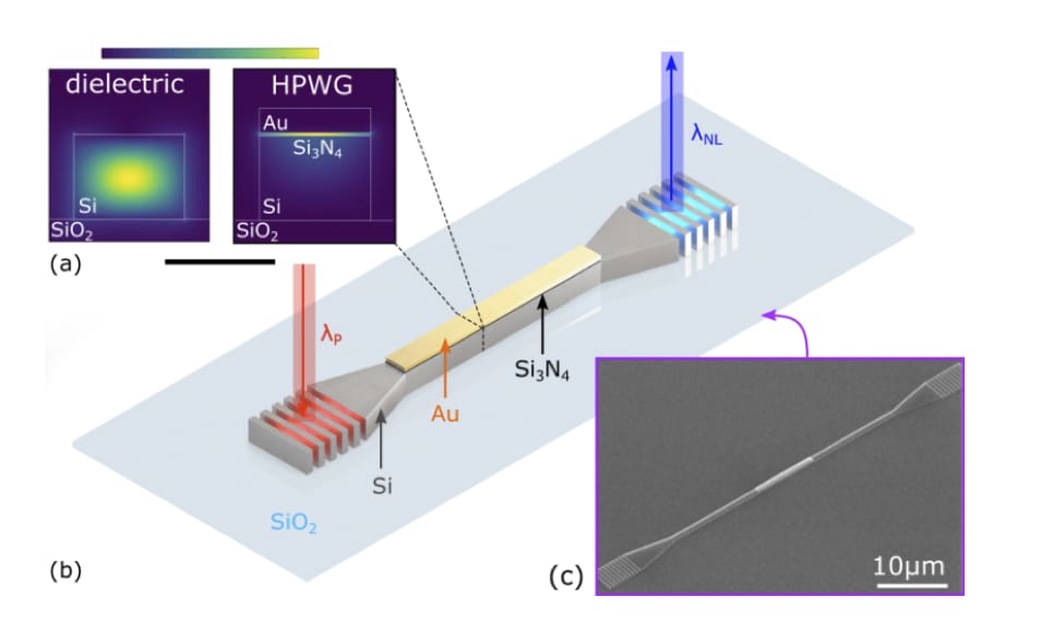
(a) Stimulation results of the power flow for the dielectric mode of a silicon waveguide (diffraction-limited confinement), and HPWG (10nm Si₃N₄ spacer), resulting in sub-wavelength confinement high intensities and low losses in the spacer. Scale bar: 350nm. λ=1550 nm.
(b) Schematic HPWG materials and operation; an input signal at a wavelength λᵖ generates a nonlinear signal at a wavelength λᶰᶫ over ~10µm.
(c) Scanning electron micrograph of a HPWG
References
- G. Li, C. M. de Sterke, S. Palomba, “Fundamental limitations of Kerr nonlinear plasmonic waveguides”, ACS Photonics, 5, 1034, (2018).
- G. Li, C. M. de Sterke, S. Palomba, “General analytic expression and numerical method for Kerr nonlinear coefficient of optical waveguides,” Opt. Lett., 42, 1329 (2017).
- G. Li, C. M. de Sterke, S. Palomba, “Figure of merit for Kerr nonlinear plasmonic waveguides”, Laser & Photonics Reviews, 10, 639 (2016).
- F. J. Diaz, G. Li, B.T. Kuhlmey, C. M. de Sterke, S. Palomba, “Kerr Effect in Hybrid Plasmonic Waveguides”, J. Opt. Soc. Am. B, 33, 957, (2016).
- F. J. Diaz, T. Hatakeyama, J. Rho, Y. Wang, K. O’Brien, X. Zhang, B.T. Kuhlmey, M. de Sterke, S. Palomba, “Sensitive method for measuring third order nonlinearities in compact dielectric and hybrid plasmonic waveguides”, Opt. Exp., 1, 545 (2016).
- T. J. Duffin, M. Nielsen, F. J. Diaz, S. Palomba, S. A. Maier, R. F. Oulton, “Degenerate four-wave mixing in silicon hybrid plasmonic waveguides”, Opt. Lett., 41, 155 (2016).
Research capabilities
The Nanophotonics and Plasmonics Advancement Lab (NPAL), located in the School of Physics, aims to develop and experimentally test the next generation of linear/nonlinear/quantum integrated photonics devices. The NPAL is a world class nanophotonic and nanoplasmonic experimental facility equipped with a state-of-the-art femtosecond-OPO laser system (Coherent) for visible and infrared experiments along with a Near Field Scanning Optical Microscope for Nano-Optic research (neaSpec) and a wide range of other vital equipment necessary to achieve breakthroughs in nanophotonics such as:
- In-house developed nano-Frequency Resolved Electrical Gating (nano-FROG): for time- and phase-resolved ultrasensitive (sub-pJ) characterisation of ultrashort pulses of light (sub-ps).
- In-house developed double Hanbury Brown and Twiss (HBT) interferometer coupled to highly sensitive single photon detectors (ID Quantique): for single-photon and correlated photon measurements, essential for any quantum optics investigation
- Commercial imaging spectrometer equipped with NIR and VIS cameras (Princeton Instruments): essential for collecting images and spectra of any device we develop.
- In-house developed LabView interface: this controls all the equipment including a nanopositioner (Mad City Lab) on a Nikon Microscope system.
Stefano Palomba

Sterke Martijn de
-
+61 2 9351 7726
-
Room 307 Physics A28