Semiconducting nanowires
Semiconducting nanowires can be efficiently produced via a bottom-up growth system known as the vapor–liquid–solid mechanism. Despite considerable investigations into the growth of these nanowires, the shallow understanding of their growth handicaps the tunability of nanowire morphology for applications.
This research project is conducted via post-analysis of as-grown InGaAs nanowires at atomic-scale, to deduce the thermodynamics of nanowire growth, specifically, chemical distribution, the geometry evolution, and crystallography. The outputs of this project are expected to be a guideline for the synthesis of the nanowires in a controllable manner for targeted application.
This project involves nanowire growth and characterisation, which are conducted via the collaboration among national organisations in Australia. The nanowires are grown in a horizontal flow Aixtron 200/4 metal organic chemical vapour deposition system (MOCVD) at the Australian National University (ANU), and the characterisation is carried out by using the facilities at the Australian Microscopy & Microanalysis Research Facility (AMMRF) and Australian Institute for Nanoscale Science and Technology (AINST) located at the University of Sydney, where the primary microscopic techniques involved in this project are CAMECA local electrode atom probe 4000XSi (APT), JEOL 2200 transmission electron microscope (TEM), Zeiss Auriga Scanning Electron microscope/focus ion beam (SEM-FIB), etc., in conjunction with first principles calculation (DFT) supported by researchers at the Australian Centre for Microscopy & Microanalysis (ACMM).
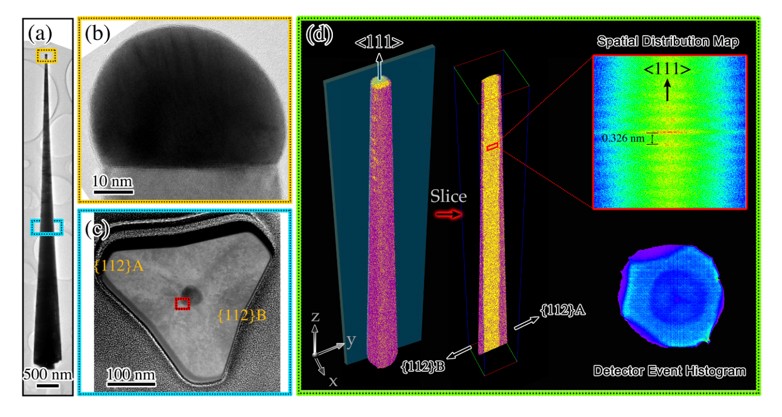
(a) BF TEM image of entire single InGaAs NW on a TEM grid with holy carbon film.
(b) High-resolution TEM (HRTEM) image at Au/NW interface.
(c) STEM image of NW cross section corresponding to the blue rectangle region in panel a shows core-shell structure.
(d) An axial slice of NW tomography sampled from InGaAs NW tomography which was indicated by blue transparent plane showing inhomogeneous shell; Ga atoms are in yellow and In in purple. Atomic spatial distribution map of NW sampled from tomography showing 0.326 nm d-space of lattice plane along <111>. And the projection of APT detector event histogram is consistent with panel c.
In their recent paper published in Advanced Materials, this project team volumetrically mapped the elements and 3D position of atoms within a single Indium-Gallium-Arsenic (InGaAs) nanowire, 50nm in diameter, by using cutting-edge APT on the centre’s CAMECA LEAP 4000Si instrument, which gives opportunity to investigate the nanowire at atomic scale and the crystallography of nanowires was studied in TEM. The tiny specimens were prepared in the SEM-FIB. Tomography revealed that the core and shell of these nanowires exhibited directional growth and that atoms migrated between the core and the shell of the structure. The team used this insight to propose a new simulated model that explained these atomic-scale 3D observations.
Such unprecedented 3D insights into nanowire structure and shape enable a deeper understanding of the relationship between nanowire growth habits, their atomic structure and how that influences their semiconducting properties, facilitating the development of nanowires for increasingly targeted applications.
Other ongoing research by Associate Professor Rongkun Zheng’s team involves characterisation of magnetic materials, biomaterials, microelectronics, etc., and straining engineering on 2D materials, energy band engineering based on first principle calculation, which has been conducted by his PhD students and postdoctoral fellows.
Besides advancing the current projects in more depth, the team’s research scope extends to other broader areas, such as catalyst and solar cells, based on advanced instruments at ACMM and Sydney Nano.
Rongkun Zheng
