
Our capabilities
Our current capabilities include:
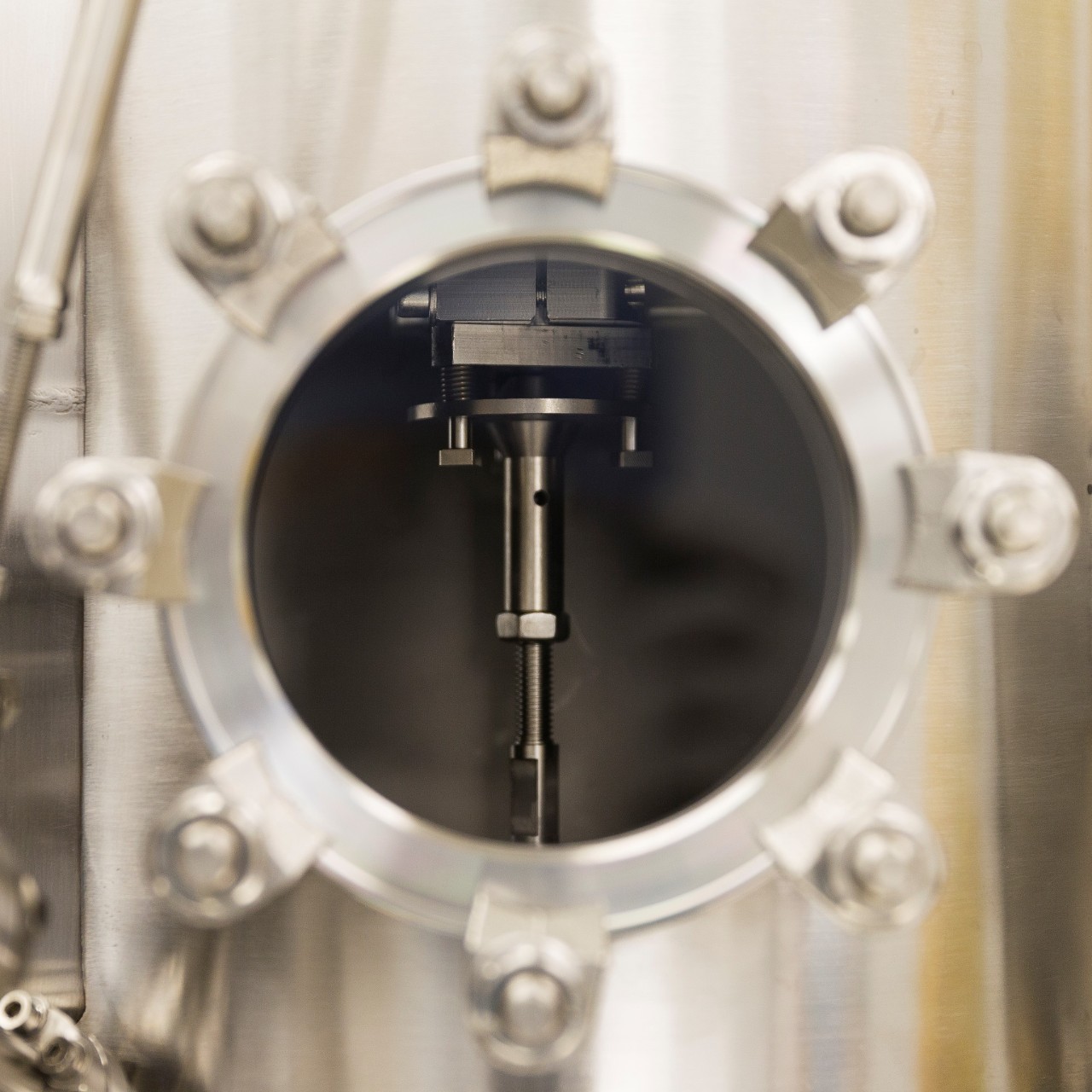
Deposition
Vacuum deposition is a family of processes used to deposit layers of material atom-by-atom or molecule-by-molecule on the surface of a substrate. The deposited layers can range from a few atomic layers to several micrometres. The films are made in a highly controlled environment and multiple materials can be combined through mixing, layering, or other means to tune the behaviour of the material. Based on the vapor source, vacuum deposition can be divided into two broad categories: physical vapor deposition (PVD) and chemical vapor deposition (CVD).
Tools: Atomic Layer Deposition Picosun R200
E-Beam/Thermal Evaporator AJA ATC-1800-E
Sputter Coater DC Emitech K550
Sputterer AJA ATC-2000-UHV
Lamp Annealer ULVAC MILA 5000
PECVD Oxford PlasmaPro 100
UHV Deposition System (Plassys MEB550S4-1)
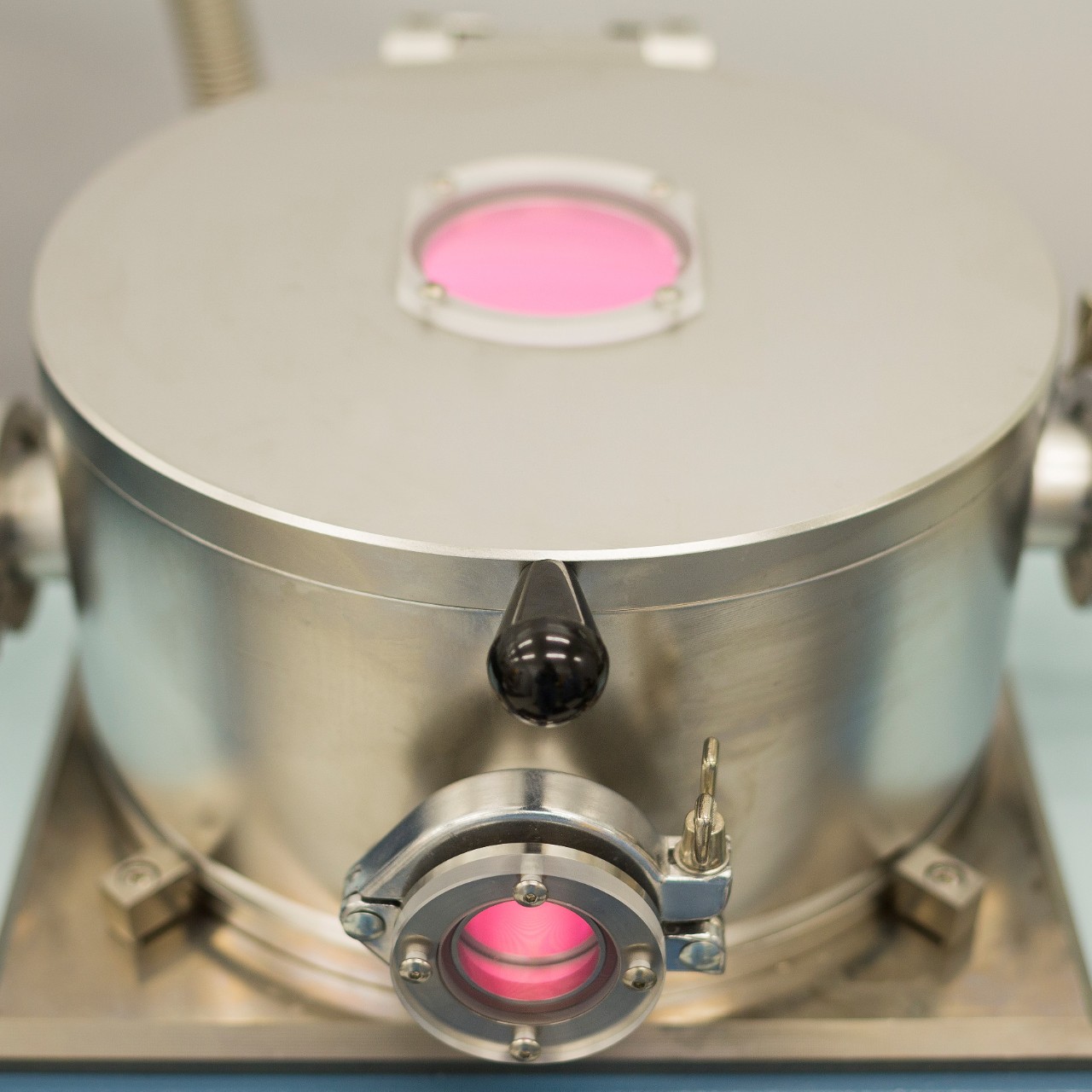
Dry etch
Micro-to-nano fabrication dry etching technology provides engineers and scientists ways to remove materials with atomic precision. With proper chemistry, reactive ion etching (RIE) removes one material rapidly while slowly etching another. This contrast enables a pattern
from a thin stencil to be transferred deep into a material, providing a desirable aspect ratio. On the other hand, a heavy gas such as argon can be blasted at the material to erode its surface, leading to a more milling effect.
Tools: ICP RIE Oxford Plasmalab 100
O2 Plasma Asher Glow
Reactive Ion Etcher (Plasmatherm Vision)
Reactive Ion Etcher (South Bay RIE3000)
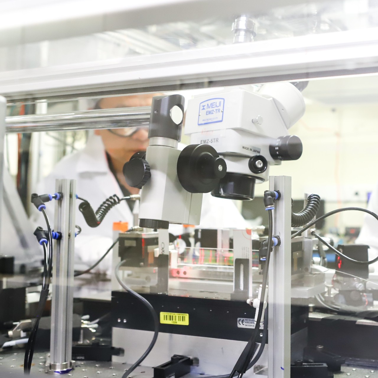
Fibre Bragg Grating facility
The Advance Fibre Bragg Grating (FBG) facility is a new inclusion to RPF facility. The FBG facility is based on technology developed and engineered for more than 20 years. The FBG facility can fabricate complicated FBG designs of arbitrary amplitude and phase with high fidelity and quality. FBGs are useful optical components for sensing, optical communications, and optical signal processing.
A FBG is constructed with index modulation fabricated on a section of fibre by UV laser exposure. A typical application is for optical filters used in optical undersea cables which accounts for 99% of data traffic that is crossing oceans. Photonic components, modules and subsystems made by FBGs, such as fibre lasers, are also widely used.
Tools: Advance Fibre Bragg Gratings
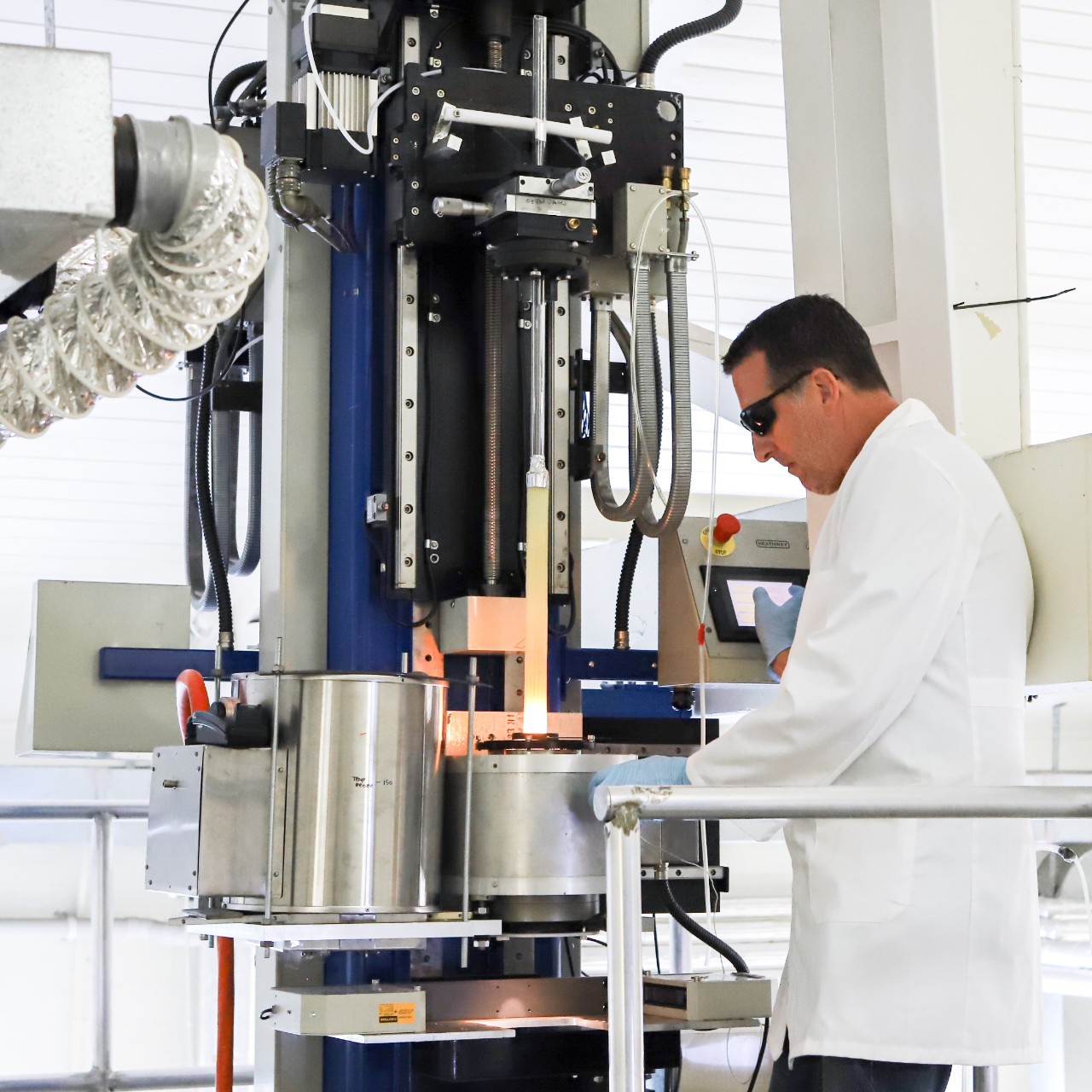
Fibre fabrication
Fibre fabrication is a process for making long uniform lengths of fibre, typically of dimensions between tens of microns
Our fibre manufacturing capabilities include polymers, soft glass, waveguides, co-drawn wires, and air or fluidic microstructures. Our manufacturing equipment includes a six-meter dual sided Heathway fibre draw tower for primary and secondary drawing with three furnace options for various preform sizes and temperature requirements. A pressurised fibre coating system, tractor draw unit for capillary / cane drawing, a pressurised drawing system, and spinning motor chuck mount for drawing spun fibres. and millimetres, and typically with complex transverse structure. This structure can provide waveguiding, or engineering mechanical, electrical, magnetic, or fluidic functionalities. It is typically a two stage process where the desired structure is assembled on macroscale, in a “preform”, and this is then drawn in a furnace down to fibre. Glasses and thermoplastics are readily drawn and can be co-drawn with some metals. The preforms may be produced by a variety of techniques including “stacking and drawing”, milling, or casting, and the fibre is drawn on a draw tower.
We run a CNC mill on site which allows us to accurately drill holes in various materials, giving us the ability to draw those materials down into fibres whilst maintaining the hole structures using internal pressure.
Tools: Fibre Draw Tower
CNC Mill
Fibre Hydrogenation System
Lithography
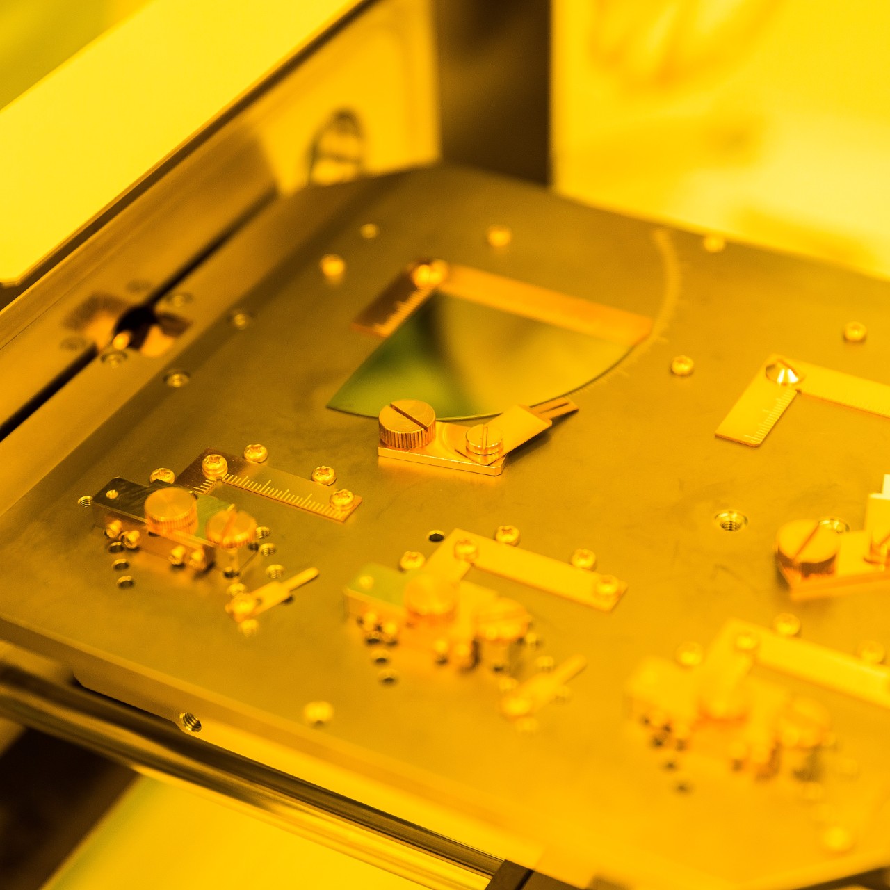
Direct laser lithography is a process used to directly transfer a design pattern into a photo sensitive polymer coated onto a substrate such as glass or silicon. The focused laser light (generally 370 or 405nm) is used to modify the polymer to make the material more soluble during development or to cross link the polymer causing it to remain during development. The advantage of this approach is that it negates the use of expensive chrome masks and speeds up the development cycle of devices. It also overcomes some of the other technical shortcomings of contact lithography such as resolution and process uniformity.
We have a suite of tools for optical lithography, as well as substantial supporting tools for spin coating and developing. The DWL66+ and MLA100 are direct write photolithography tools, allowing the exposure process to be done without the use of a photomask.
Electron Beam Lithography (EBL) allows users to write patterns with extremely high resolution, smaller than 10nm in size. Due to the high-resolution nature of the technique, EBL has a vast range of applications including nano-electronics, photonics, plasmonics, nano-fluidics, MEMS, x-ray, and neutron optics.
Tools: Dry Film Laminator Fortex FL-0305-01
EBL Elionix ELS-F125
Laser Writer Heidelberg DWL 66+
Mask Aligner EVG 610
Maskless Aligner Heidelberg MLA100
3D Microprinting Nanoscribe PPGT2
Wafer coater and developer Picotrack PCT-150
Metrology
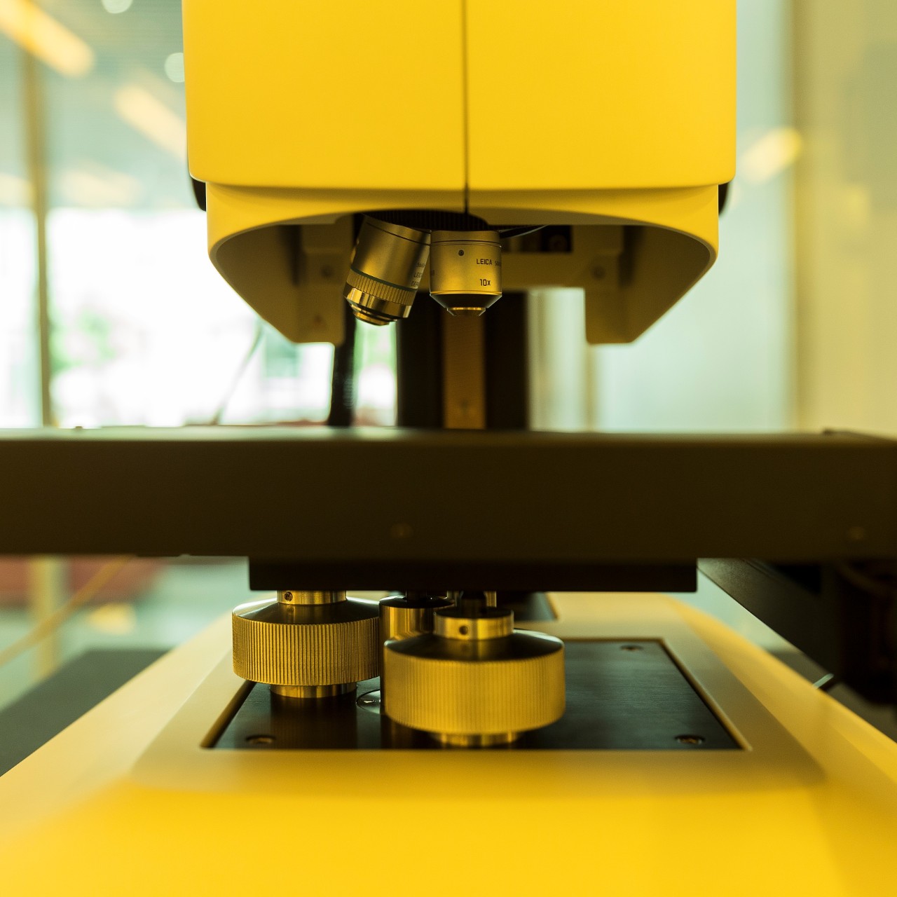
Metrology is a critical part of the fabrication process, allowing verification of design, processes, and functionality. The RPF’s current capability includes two high-end scanning beam systems, Nanofab Helium Ion Beam and FIB-SEM, from Zeiss, as well as Bruker Atomic Force Microscope, DekTak Stylus Profilometer, a Leica DCM8 3D microscope, a Reflectometer, an Ellipsometer, a number of optical microscopes, and electrical testing probe stations.
Scanning Electron Microscopy (SEM) is the process whereby a tightly focused electron beam is scanned onto the surface to be imaged. SEM is a key tool for process characterisation of surface topography, cross-section profiles, elemental composition, and crystallography. Atomic force microscopy (AFM) is a versatile technology consisting of many characterisation methods. AFM performs scanning probe microscopy, scanning the surface of a material with a nanoscale cantilever, either through direct contact or through oscillating the cantilever just above the surface. AFM has a wide range of applications including nanoscale materials and surface characterisation, electrical materials characterisation, interaction forces and mechanical properties mapping. The Reflectometer and Ellipsometer offer characterisation of thin films, while optical microscopy uses a series of lenses to focus light that is reflected from or passed through a sample; various forms of light and magnification can be used to visualise the sample. Probe stations characterise electrical properties and device functionality.
Tools: 3D Microscope Leica DCM8
Atomic Force Microscope Bruker Icon
Ellipsometer JA Woollam M2000
FIB-SEM Zeiss Crossbeam 550XL
Microscope Nikon Eclipse LV100ND
Digital Microscope Olympus DSX510
NanoFab Helium Ion Beam Zeiss
Stylus Profilometer DekTak XT
Desktop SEM Phenom XL
Parametric analyser Keithley
Semi-automatic 150mm wafer prober Semiprobe
Thin film stress measurement MOS Ultrascan
Packaging
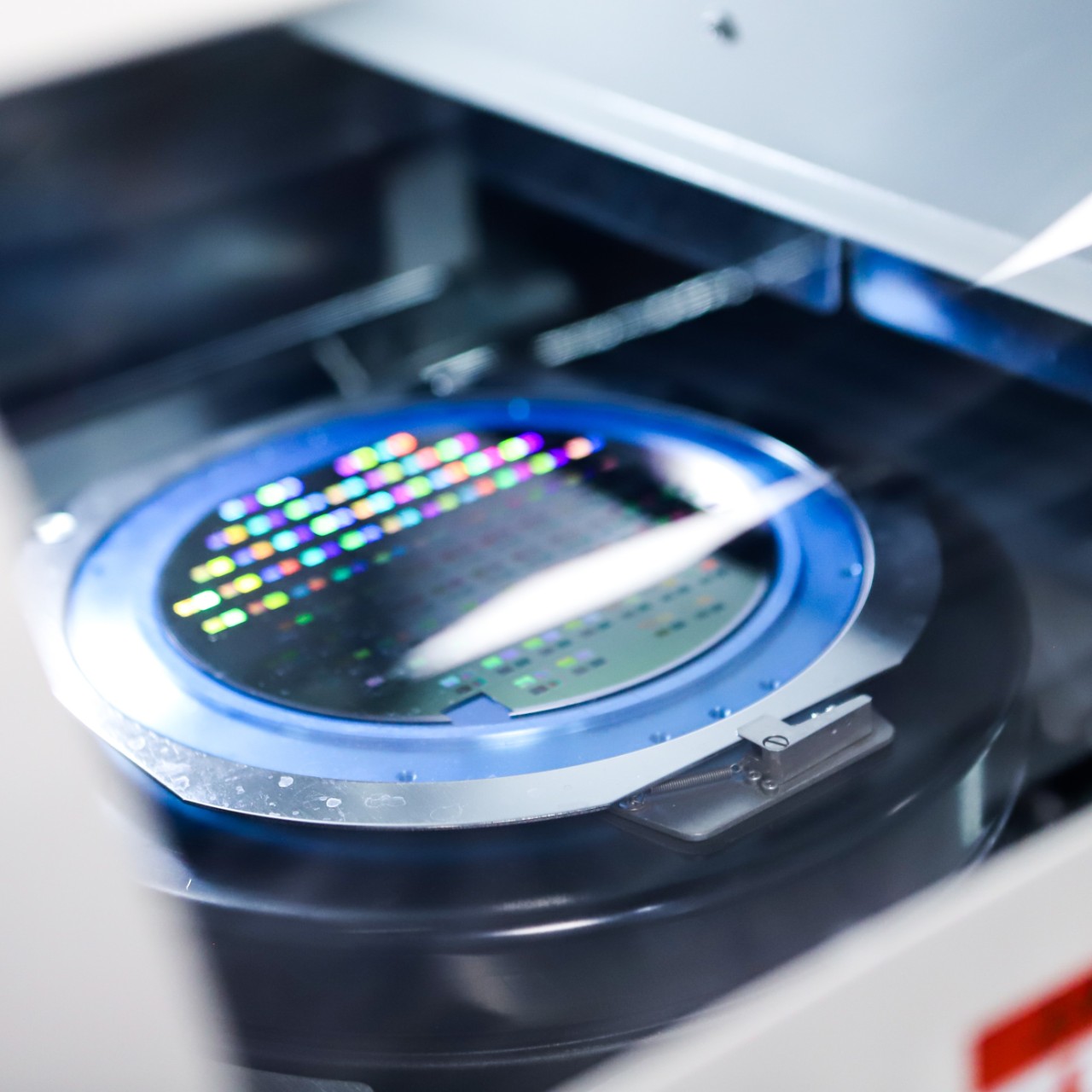
Device packaging is the final step in the fabrication process. Packaging of a micro- or nano-electrical device allows components to be operated in applied environments by providing mechanical stability and functionality. Wire bonding allows nanoscale electrical components to communicate with the outside world, with thin electrically conductive wires allowing electricity to flow from contacts on the component to, or from, its packaging. Bonding a wafer to another wafer can help a form new functions in a device or can ensure mechanical and hermetic encapsulation of devices and electronics. Other packaging tools include dicing saws, used to separate nanofabricated devices, and probe stations, used to electrically probe nanoscale electrical components prior to mechanical and electrical packaging.
Tools: Dicing Saw ADT 7122
Die Bonder Finetech Lambda
Probe Station Suss PM 5
Wire Bonder TPT HB100
Desktop PCB Printer BotFactory
Semiautomatic Die Bonder TPT HB 75
Photomask fabrication service
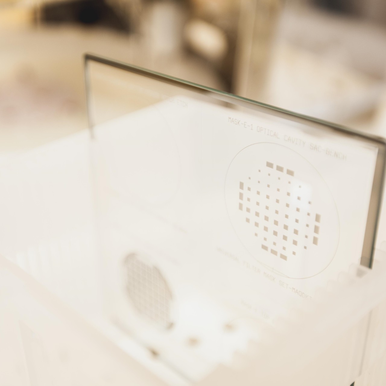
The RPF provides full service for chrome-glass photomask fabrication with client's design and requirements. Photolithography is used to create a pattern on a substrate by shining light from a light source onto a photoresist that coats the surface of the substrate through a photomask and is followed by a development phase. Depending on the complexity of a device’s design, various deposition, etching, and lithography processes can be cycled through many times. Each mask used must be aligned perfectly to the previously processed layer if the final device is to operate as desired.
Soft lithography
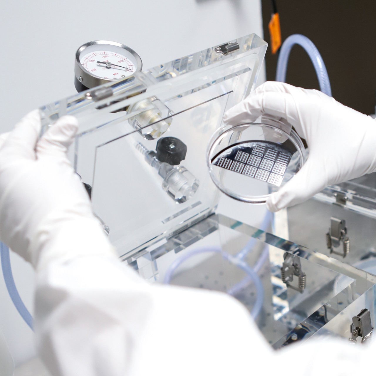
Soft lithography is a technique used to imprint structures into mechanically soft materials from a master mould or stamp. This method of pattern transfer is used to make microfluidic devices for applications which require biocompatible materials such as Polydimethylsiloxane (PDMS). Equipment includes spin coaters (for thin layers), ovens, mixers and casting equipment.
Tools: Coater Brewer Science CB-200
PDMS Process Tools
Wet processing
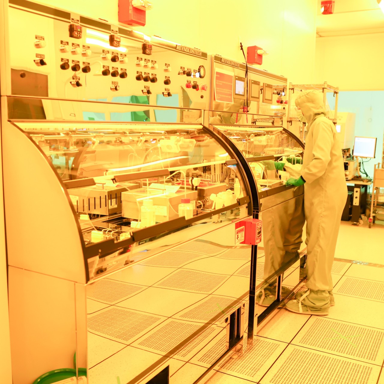
The fabrication of micro and nanoscale devices requires the use of many wet chemical processes. Wet processing encompasses the processing of chemicals to clean, deposit material onto, and etch material away from substrates and components. Wet benches allow users to access solvent, caustic, and acid-based processing in a safe and dedicated environment.
Tools: Electroplating Technic Inc
uEtch HF vapour etch SPTS
Chemical mechanical polishing Alpsitec E400
Spin rinse dryers OEM
Solvent benches (resist coat & develop) Reynolds Tech
Wet Benches (acid & caustic) Reynolds Tech
Look inside the facility
See how we enable micro- and nano-scale fabrication.